DATA SHEET
Product specification
File under Integrated Circuits, IC04
January 1995
INTEGRATED CIRCUITS
HEF4066B
gates
Quadruple bilateral switches
For a complete data sheet, please also download:
The IC04 LOCMOS HE4000B Logic
Family Specifications HEF, HEC
The IC04 LOCMOS HE4000B Logic
Package Outlines/Information HEF, HEC
January 19952
Philips SemiconductorsProduct specification
Quadruple bilateral switches
HEF4066B
gates
DESCRIPTION
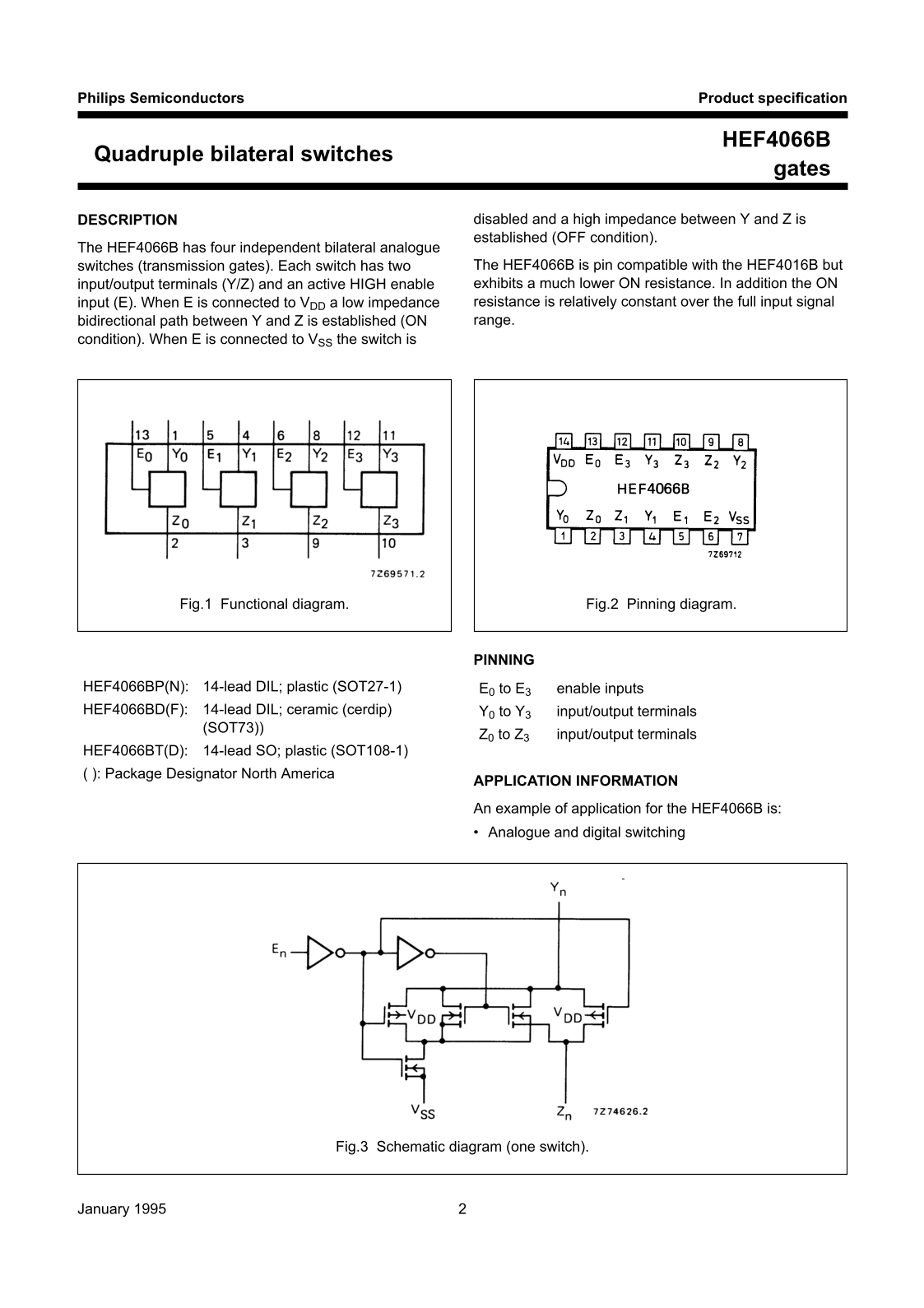
The HEF4066B has four independent bilateral analogue
switches (transmission gates). Each switch has two
input/output terminals (Y/Z) and an active HIGH enable
input (E). When E is connected to V
DD a low impedance
bidirectional path between Y and Z is established (ON
condition). When E is connected to V
SS the switch is
disabled and a high impedance between Y and Z is
established (OFF condition).
The HEF4066B is pin compatible with the HEF4016B but
exhibits a much lower ON resistance. In addition the ON
resistance is relatively constant over the full input signal
range.
Fig.1 Functional diagram.Fig.2 Pinning diagram.
HEF4066BP(N): 14-lead DIL; plastic (SOT27-1)
HEF4066BD(F): 14-lead DIL; ceramic (cerdip)
(SOT73))
HEF4066BT(D): 14-lead SO; plastic (SOT108-1)
( ): Package Designator North America
PINNING
APPLICATION INFORMATION
An example of application for the HEF4066B is:
Analogue and digital switching
E
0 to E
3 enable inputs
Y
0 to Y
3 input/output terminals
Z
0 to Z
3 input/output terminals
Fig.3 Schematic diagram (one switch).
Previous Page Next Page