January 19952
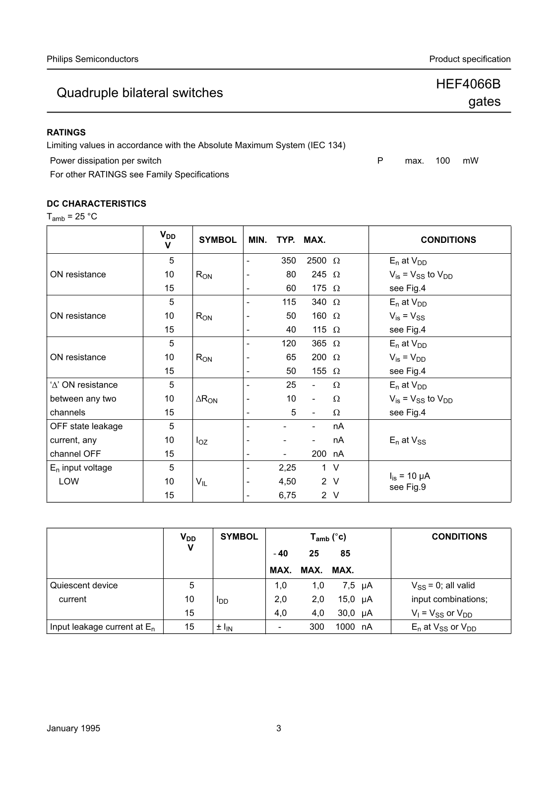
Philips SemiconductorsProduct specification
Quadruple bilateral switches
HEF4066B
gates
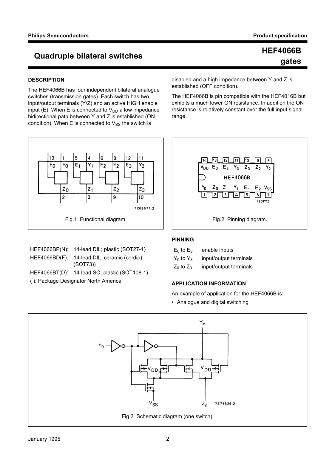
DESCRIPTION
The HEF4066B has four independent bilateral analogue
switches (transmission gates). Each switch has two
input/output terminals (Y/Z) and an active HIGH enable
input (E). When E is connected to V
DD a low impedance
bidirectional path between Y and Z is established (ON
condition). When E is connected to V
SS the switch is
disabled and a high impedance between Y and Z is
established (OFF condition).
The HEF4066B is pin compatible with the HEF4016B but
exhibits a much lower ON resistance. In addition the ON
resistance is relatively constant over the full input signal
range.
Fig.1 Functional diagram.Fig.2 Pinning diagram.
HEF4066BP(N): 14-lead DIL; plastic (SOT27-1)
HEF4066BD(F): 14-lead DIL; ceramic (cerdip)
(SOT73))
HEF4066BT(D): 14-lead SO; plastic (SOT108-1)
( ): Package Designator North America
PINNING
APPLICATION INFORMATION
An example of application for the HEF4066B is:
• Analogue and digital switching
E
0 to E
3 enable inputs
Y
0 to Y
3 input/output terminals
Z
0 to Z
3 input/output terminals
Fig.3 Schematic diagram (one switch).
Philips SemiconductorsProduct specification
Quadruple bilateral switches
HEF4066B
gates
DESCRIPTION
The HEF4066B has four independent bilateral analogue
switches (transmission gates). Each switch has two
input/output terminals (Y/Z) and an active HIGH enable
input (E). When E is connected to V
DD a low impedance
bidirectional path between Y and Z is established (ON
condition). When E is connected to V
SS the switch is
disabled and a high impedance between Y and Z is
established (OFF condition).
The HEF4066B is pin compatible with the HEF4016B but
exhibits a much lower ON resistance. In addition the ON
resistance is relatively constant over the full input signal
range.
Fig.1 Functional diagram.Fig.2 Pinning diagram.
HEF4066BP(N): 14-lead DIL; plastic (SOT27-1)
HEF4066BD(F): 14-lead DIL; ceramic (cerdip)
(SOT73))
HEF4066BT(D): 14-lead SO; plastic (SOT108-1)
( ): Package Designator North America
PINNING
APPLICATION INFORMATION
An example of application for the HEF4066B is:
• Analogue and digital switching
E
0 to E
3 enable inputs
Y
0 to Y
3 input/output terminals
Z
0 to Z
3 input/output terminals
Fig.3 Schematic diagram (one switch).