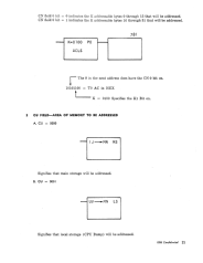
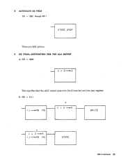
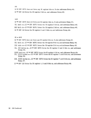
5 bit will be set on (1). If the Low 4 bits of the Z buss are not zeroes, the S
register 5 bit will be reset off (0). (See example 13A, page 29.)
C5
=
0010
(HZ~
54)
This specifies that if the High 4 bits of the Z buss are zeros, the S register
4 bit will be set on (1). If the High 4 bits of the Z buss are not zeros, the S
register 4 bit will be reset off (0). (See example 13A, page 29.)
CS
=
0011
(LZ~
55,
HZ~
54)
This specifies that if the High-Low 4 bits of the Z buss are zeros or any
combination thereof, the corresponding S register 4 and 5 bits will be set
on (1). If the High-Low 4 bits of the Z buss are not zeroes or any combina-
tion thereof, the corresponding S register 4 and 5 bits will be reset off (0).
(See example 13A, page 29.)
C5
=
0100 (0
~
54, 55)
This specifies that the S register 4 and 5 bits will be reset off (0).
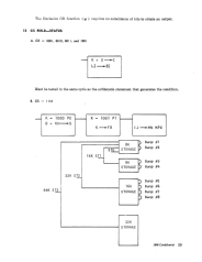
CS
=
0101 (Treq
~
51)
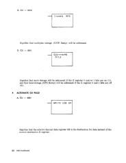
This specifies that if a 1050 request occurs, the S register 1 bit will be set
on
(1).
C5
=
0110
(O~
50)
This specifies that the S register
0
bit (true-complement latch) will be re-
set off (0).
C5
=
0111
(I
~
50)
This specifies that the S register 0 bit (true-complement latch) will be set
on (1).
C5 = 1000
(O~
52)
This specifies that the S register 2 bit will be reset off (0).
C5
=
1001
(ANSNZ~52)
This specifies that if the Z buss (results of an arithmetic statement) is non-
zero, the S register 2 bit will be set on (1). If the Z buss is zero, the S reg-
ister 2 bit would not be reset. (See example 13A, page 29.)
NOTE
A special function of the above decode takes place if the
suppress-machine trap latch is on (1), the CPU check
switch is in diagnostic mode, and the Z buss is not zero (0);
the machine is forced to a hard stop.
C5 = 1010 (0
~
56)
This specifies that the S register 6 bit will be reset off (0).
CS
=
1011 (I
~
56)
This specifies that the S register 6 bit will be set on (1).
C5
=
1100 (0
~
57)
This specifies that the S register 7 bit will be reset off (0).
C5
=
1101
(I~57)
This specifies that the S register 7 bit will be set on (1).
C5
=
1110 (K
~
FB)
This specifies the controls for numerous MPX channel conditions.
K - 1100 PI-Sets the MPX channel interrupt latch on.
K = 0110 PI-Sets the MPX operation latch on.
IBM
ConfiJ~ntitll
13