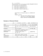
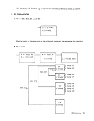
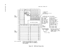
c.
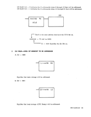
CU - 0010
- T-N MPX
Signifies that multiplex storage (UCW Bump) will be addressed.
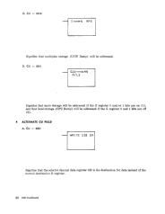
D. CU - 0011
- GUV-MN
M/LS
Signifies that main storage will be addressed if the G register 0 and/or 1 bits are on (1),
and that local storage (CPU Bump) will be addressed if the G register 0 and 1 bits are off
(0) •
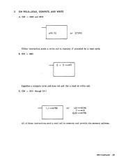
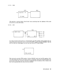
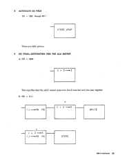
4 ALTERNATE CU FIELD
A. CU
=
0001
- WRITE USE GR
Signifies that the selector channel data register GR is the destination for data instead of the
normal destination R register.
22
IBM
Confidential