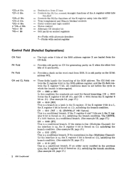
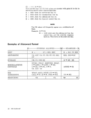
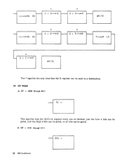
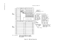
CM Field
SEL 1, SEL 2, EXT., TIMER are up, the X register 7 bit is forced on (1),
satisfying the branch condition. (See example 1B, page 17.)
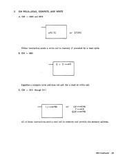
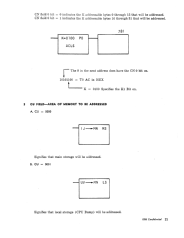
This field controls the reading and the writing of memory.
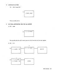
CM
= 0000 (Write)
This decode sends a write call to memory.
It
resets the allow write latch.
If
one write follows another write, the second write is ignored because the al-
low write latch was reset by the first write operation.
If
the write follows a
read, the data read will set into R register and be regenerated. (See exam-
ple
2A,
page 19.)
CM
=
0001 (Compute)
This decode asks for neither a read nor write call. This decode can be used
for generating new R register data which will be written back, with either
a write or store, during the next cycle. (See example 2B, page 19.)
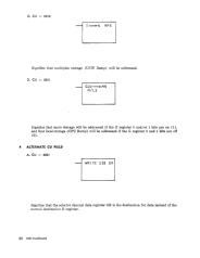
CM
= 0010 (Store)
This decode sends a write call to memory.
It
also resets the allow write
latch.
If
the store follows a read, the DATA READ WILL NOT be set into
the R register, but what is already in the R register will be regenerated.
(See example
2A,
page 19.) .
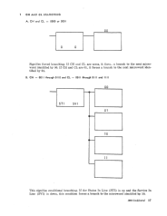
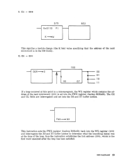
CM = 0011
(IJ~
MN)
This decode sends a read call to memory and specifies an address for the
memory address MN register.
It
turns on the allow write latch and gates
the IJ register address to the MN register.
It
also addresses that location
of either the main storage or local storage. The data from the addressed
location is read out and into the R register.
If
one read follows another
read, the second read is ignored (no read call), but the IJ address is gated
to the MN register. (See example 2C, page 19.)
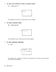
CM = 0100 (UV~ MN)'
This decode sends a read call to memory and specifies an address for the
MN register. This decode turns on the allow write latch and gates the UV
register address to the MN register and addresses that location of either
the main storage or the local storage. The data from the addressed location
is read out and into the R register.
If
one read follows another read, the
second read is ignored (no read call), but the UV address is gated to the
MN register. (See example 2C, page 19.)
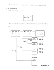
CM
=
0101
(T~
N)
This decode sends a read call to memory and specifies an address for the Lo
order 8 bits of the MN register. This decode turns on the allow write latch
. and gates the T register address to the N register (the M register is reset).
It
addresses that location of either the main storage or the local storage.
The data from the addressed location is read out and into the R register.
If
in the 1401 mode, it gates the LT register address to the MN register.
If
one read follows another read, the second read is ignored (no read call),
but the T or LT address is gated to the N or MN register. (See example
2C, page 19.)
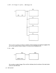
CM
=
0110 (hhl)
This decode sends a read call to memory and specifies an address for the
MN register.
It
turns on the allow write latch and gates the HEX address
of one of the local storage coordinates (determined by the CK field and CN
field next address) to the MN register. The decode addresses that location
of the local storage. The data from the addressed location is read out and
into the R register. If one read follows another read, the second read is ig-
nored (no read call), but the HEX address is gated to the MN register.
(See example 2D, page 20.)
IBM Con/iJentil,z
5 .