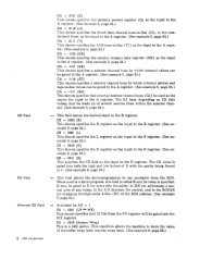
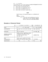
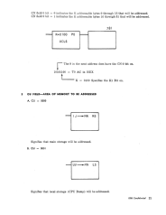
D. eM
=
0110
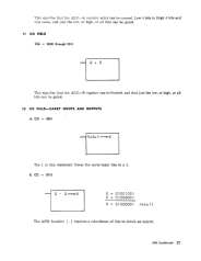
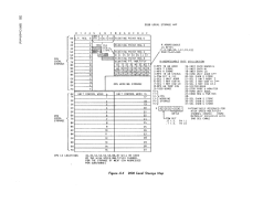
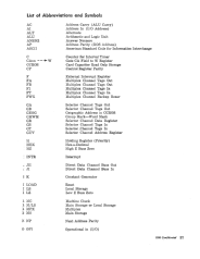
This illustrates how the K addressable byte is formed.
OX
IX
2X
3X
4X
5X
6X
7X
8X
9X
AX
BX
CX
OX
EX
FX
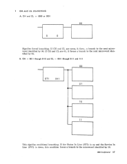
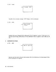
CN
BUMP MAP
0
I
2
3
4
5 6
7 8
9
A B C
0
E
F
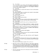
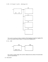
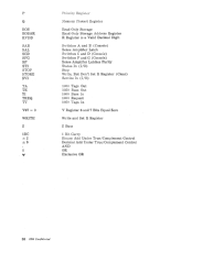
G. P. REG. 0
I NT.
I I I
STA. X X+l X+2 FLOATING PT. REG. 0
1
\
/
2
1050'Use·
FLOATING PT. REG. 2
3
4 FLOATI NG
PT. REG. 4
5
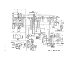
CPU
0
L
S
V
U G
J
I
6
Stored
FLOATING
PT. REG.
6
7
FLOAT I NG PT MULTIPLY
8
0
1
2
3
4
5
6
7
9
8
9
10
1 1 12
13
14 15
10
16
17
18
19
20 21
22
23
I I
24 25 26 2] 28 29
30
.l.L ....
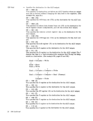
12
11
14
CPU WORKING STORAGE
15
rlFORCEO ON
IFORCEO
OFF
rFORCEO
ON
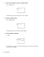
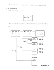
1 0 CNO KO 1 KI K2
K3
l-
K ADDRESSABLE
BUMP BYTES
(I,O,CNO,KO,I,
Kl,K2,K3)
FIELD 0
BIT~
t
r
t
t
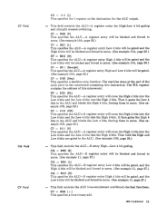
SPECIFIED BY CK FIELD
rr
These two dig its of the HEX
address are derived from the
CN field plus the X6 and X7
76 1 bits.
1I..-.-----J
K
;A 00
~~
PO
11'--------' I
The CN 0,1,2,3 bits
The CN 4,5,6,7 bits
=
6(0110)
1
(000 1 )
~The
6 in the next
1000 1010
=
TO 8A in HEX
address does not have the CN
a
bit on.
1L-____
K
=
0010 spec i fi es the K2 bi ton.
20
IBM COllfidl!lltial