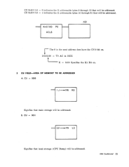
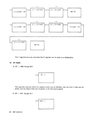
CB Field
CK Field
Alternate CK Field
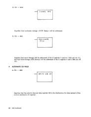
8
IBM COll/idl'1ltial
CA
=
0101
(9)
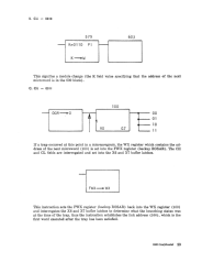
This decode specifies the memory protect register
(Q)
as the input to the
A register. (See example 5, page 24.)
CA
=
0110
(Jq
This decode specifies the direct data channel buss-in-line (JI), in the com-
plement form, as the input to the A register. (See example 5, page 24.)
CA = 0111 (TI)
This decode specifies the 1505 buss-in-line (TI) as the input to the A regis-
ter. (See example 5, page 24.)
CA
=
1100 (GR)
This decode specifies the selector channel data register (GR) as the input
to the A register. (See example 5, page 24.)
CA
=
1101 (GS)
This decode specifies a selector channel buss by which internal values can
be gated to the A register. (See example 5, page 24.)
CA
=
1110 (GT)
This decode specifies a selector channel buss by which internal latches and
tags-in-line values can be gated to the A register. (See example 5, page 24.)
CA = 1111 (GJ)
This decode specifies that internal selector channel buss (GJ) be used as the
source for input to the A register. The GJ buss, depending on CK field
values, may be made up of several sources from within the selector chan-
nel. (See example 5, page 24.)
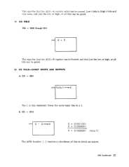
This field names the desired input to the B register.
CB
=
0000 (R)
This decode specifies the R register as the input to the B register. (See ex-
ample 6, page 24.)
CB
=
0001 (L)
This decode specifies the L register as the input to the B register. (See ex-
ample 6, page 24.)
CB
=
0010 (0)
This decode specifies the D register as the input to the B register. (See ex-
ample 6, page 24.)
CB
=
0011 (K)
This specifies the CK field as the input to the B register. The CK value is
gated into both the high and low halves of B with the parity being forced
to
1.
(See example 6, page 24.)
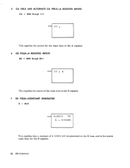
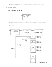
This field allows the microprogrammer to use constants from the ROS.
When used in a microprogram, this field is called K and its value is specified.
K may be gated to B for entry into the adder, to MN for addressing a spe-
cial area of any bump, to the I/O channels for control, and to the ROSAR
for changing the high-order 4 bits (W) of the ROS address. (See example
7, page 24.)
Activated by AK
=
1
CK
=
0001
(UV~
WX)
This decode specifies that 12 bits from the UV register will be gated into the
WX register.
CK
=
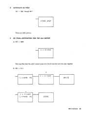
0010 (Restore Wrap)
This is a 64K option. This condition allows the machine to store the value
of the buffer wrap latch into the wrap latch. (See example 8, page 25.)