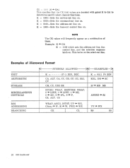
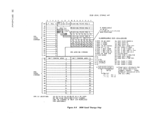
CU Field
Alternate CU Field
CA Field
6
IBM Confidential
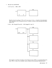
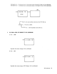
CM
=
0111
(GUV~
MN)
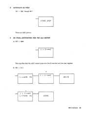
This decode sends a read call to memory and specifies an address for the
MN register. This decode turns on the allow write latch and gates the GUY
(selector channel) register address to the MN register.
It
also addresses that
location of either the main storage or the local storage. The data from the
addressed location is read out and into the R register.
If
one read follows
another read, the second read is ignored (no read call), but the GUY ad-
dress is gated to the MN register. (See example 2C, page 19.)
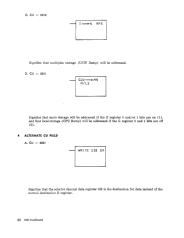
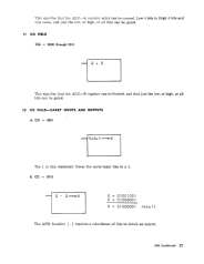
This field specifies the area of memory to be addressed (MS, LS and MPX),
depending on the value of the CM field.
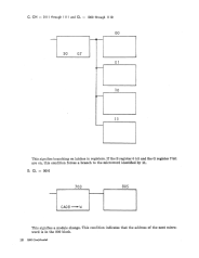
CU ..:.- 0000 (MS)
If
the CM decode is any combination of conditions 3 through 7, it specifies
that the machine is addressing the main storage. The R register is assumed
to be the destination for the data from memory. (See example 3A, page 21.)
CU
=
0001
(LS)
If
the CM decode is any combination of conditions 3 through 7, it specifies
that the machine is addressing local storage (CPU Bump). The R register
is assumed to be the destination for the data from memory. (See example
3B, page 21.)
CU
=
0010
(MPX)
If
the CM decode is any combination of conditions 3 through 7, it specifies
that the machine is addressing MPX (UCW Bump). The R register is as-
sumed to be the destination for the data from memory. (See example 3C,
page 22.)
CU
=
0011
(MILS)
This decode is a function of the macroinstruction format and specifies the
LS (CPU Bump) if the G register 0 and 1 bits are off (0).
If
either the G
register 0 and/or 1 bits are on (1), main storage is selected. The R register
is assumed to be the destination for data from memory. (See example 3D,
page 22.)
Activated by CM
=
0000,0001 or 0010.
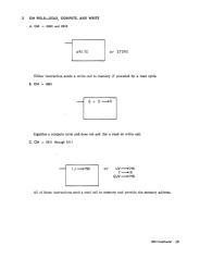
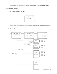
CU = 0001 (Use GR)
This decode specifies that the selector channel data register (GR) will be
the destination for data from memory. (See example
4A,
page 22.)
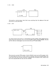
CU
=
0010
(K~W)
This decode is used for changing modules.
It
uses the CK field to specify the
value.
It
does not change the W3 bit. (See example 4B, page 23.)
CU
=
0011
(FWX~WX)
This decode gates the FWX register (backup ROSAR) into the WX regis-
ter (ROSAR).
It
restores the link address of a microprogram routine dis-
rupted by an I/O trap. (ROSAR-Read Only Storage Address Register.)
(See example 4C, page 23.)
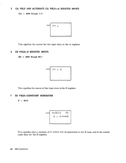
This field names the desired input to the A register.
CA
=
0000
(FT)
This decode specifies the MPX tags-in-buss (FT) as the input to the A reg-
ister. The A register parity check is blocked. (See example 5, page 24.)
CA
=
000 I (TT)
This decode specifies the 1050 tags-in-buss (TT) as the input to the A reg-
ister. The A register parity check is blocked. (See example 5, page 24.)