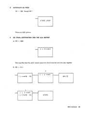
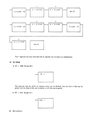
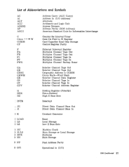
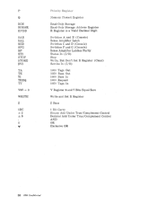
CC
Field
C5
Field
12
IBM COllfidClltill/
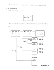
CV
=
0001 (-)
This specifies a complement binary add. The B register data is comple-
mented at the ALD-B register entry.
CV
=
00 I 0 (+ 2)
This specifies a binary add under true-complement control. This is de-
pendent on the SO bit which is the true-complement latch.
SO
=
0-True add.
SO
=
I-Complement add.
CV
=
00 I I (± 3)
This specifies a decimal add under true-complement control. This is de-
pendent on the SO bit which is the true-complement latch.
SO 0-True add.
SO
=
I-Complement add.
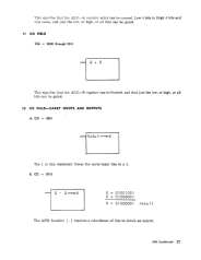
This field controls the carry inputs and outputs of the ALD and the logic
functions (AND, OR, XOR).
CC = 0000 (0)
This decode specifies that the carry-input line is to be 0 and ignores the
carry out of the ALD.
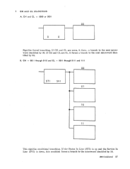
CC
=
0001
(II
This decode specifies that the carry-input line is to be 1, and ignores the
carry out of the ALD. (See example I2A, page 27.)
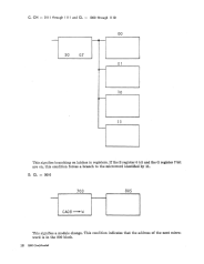
CC
=;=
00 I 0 (.)
This decode specifies the AND function and ignores the carry out of the
ALD. The AND function requires a coincidence of bits to obtain an output.
(See example I2B, page 27.)
CC
=
0011 (0)
This decode specifies the OR function and ignores the carry out of the ALD.
The OR function requires a bit on either side to obtain an output. (See ex-
ample I2C, page 28.)
CC
=
0100 (0 C)
This decode specifies that the carry-input line is to be 0 and sets the S3 bit
to 1 if a carry results. The S3 bit is the carry latch. (See example I2D,
page 28.)
CC
=
0 I 0 I (I C)
This decode specifies that the carry-input line is to be 1 and sets the S3 bit
to 1 if a carry results. The S3 bit is the carry latch.
CC
=
0110 (C C)
This decode specifies the value of the carry latch onto the carry-input line
. and sets the S3 bit to 1 if a carry results. The S3 bit is the carry latch. (See
example I2E, page 28.)
CC = 0111 (V)
This decode specifies the XOR (Exclusive OR) function and ignores the
carry out of the ALD. The XOR function requires no coincidence of bits
to obtain an output. (See example I2F, page 28.)
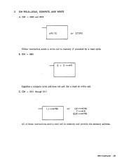
This field controls the individual sets and resets of status in the S register.
It
also controls some I/O lines. CS has an alternate decoder activated by
the bit AS
=
1.
C5 = 0001
(LZ~
55)
This specifies that if the Low 4 bits of the Z buss are zeros, the S register