VM370 Rel 6 Data Areas and Control Block Logic (Mar79)
Page30(30 of 342)
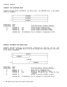
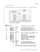
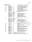
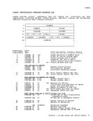
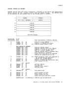
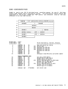
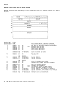
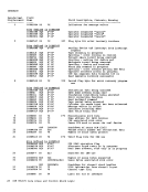
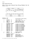
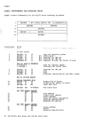
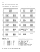
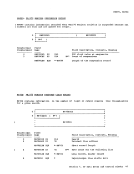
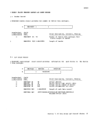
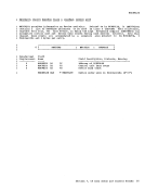
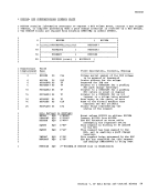
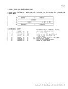
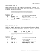
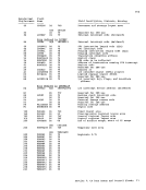
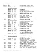
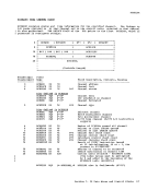
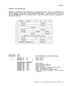
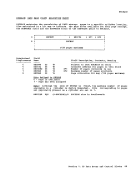
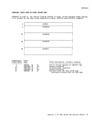
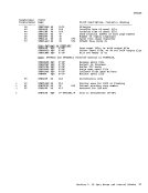
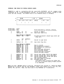
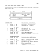
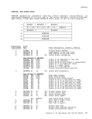
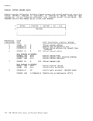
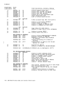
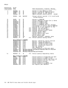
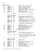
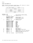
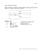
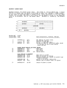
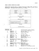
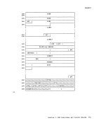
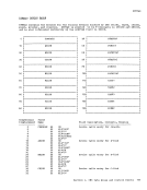
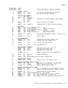
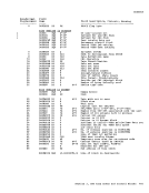
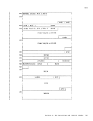
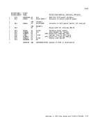
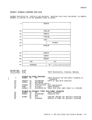
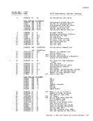
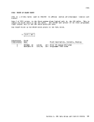
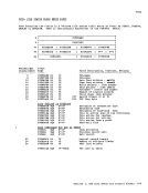
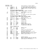
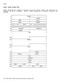
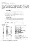
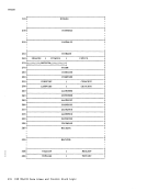
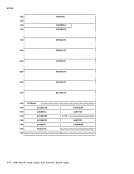
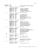
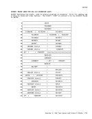
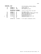
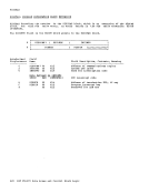
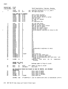
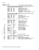
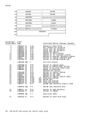
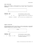
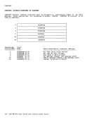
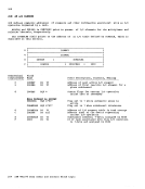
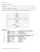
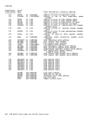
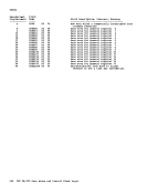
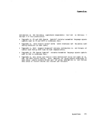
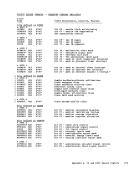
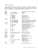
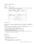
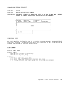
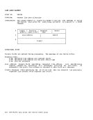
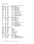
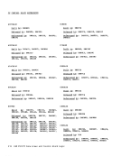
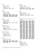
CPEXBLOK CPEXBLOK maintains register values and addressing infor.ation (module address or entry point address) to handle a delayed transfer of centrol. Stacked CPEXELCKs are queued off DMKDSPRQ. o 8 10 Hexadecimal Displacement ------------ 0 4 8 C 10 10 14 18 1C 20 24 28 2C 30 34 38 3C 40 44 48 4C CPEXFPNT CPEXMISC Field Nalle CPEXFPNT DS CPEXBPNT DS CPEXMISC DS CPEXREGS 1F 1F 1F CPIXBPNT CPIXADD Field Description, contents, !eaning Pointer to next CPEXBLCK Pointer to previous CPEXBLCK Use varies with stacker Defin!!!2] and DMKDSP ORG CPEXMISC CPEXTYPE DS 1X Type of block on CPEXBLOK chain CP_RXDEFR _EQU CPEXPRIO EQU CPEXLPSi EQU DS CPEXPROC DS CPEXADD DS CPEXREGS DS !2! CPEXRO CPEXR1 CPEXR2 CPEXR3 CPEXR4 CPEXR5 CPEXR6 CPEXR7 CPEXR8 CPEXR9 CPEXR10 CPEXR11 CPEIR12 CPEXR13 CPEIR14 CPEIR15 ORG DS DS DS DS DS DS DS DS DS DS DS DS DS DS DS DS CPEXSIZE EQU in CPEITYPE -X'80' X'40' X'20' 1X 18 IF 16F CPEXREGS 1F IF 1F 1F IF 1F IF 1F IF 1F IF 1F 1F 1F IF 1F Deferred interrupt request CPEXELOK with priority Load PSi to go to execution address Reserved for IBM use Address of processor related to block Return address Execute registers Registers 0 through 15 (*-CPEXBLOK)/8 Size in doutlewords (X'OA') 18 IBM VM/370 Data Areas and Control Block Logic
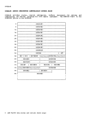
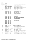
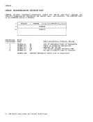
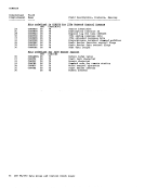
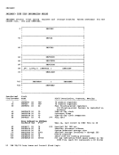
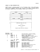
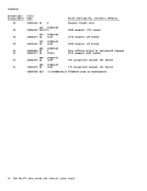
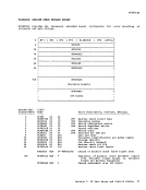
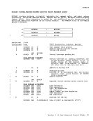
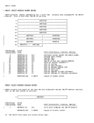
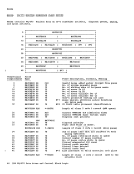
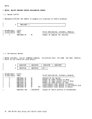
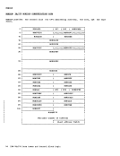
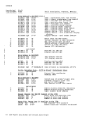
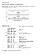
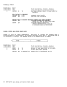
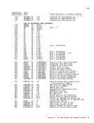
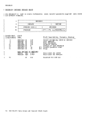
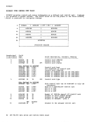
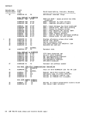
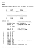
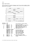
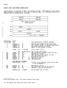
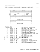
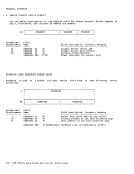
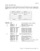
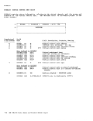
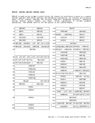
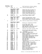
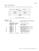
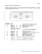
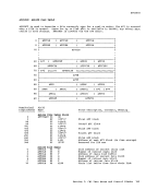
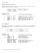
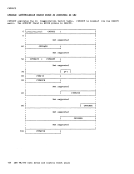
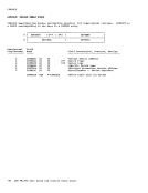
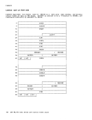
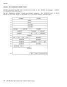
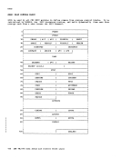
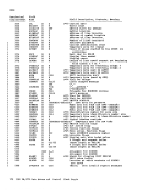
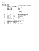
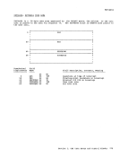
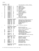
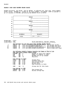
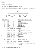
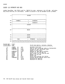
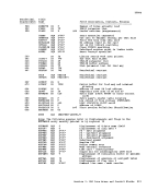
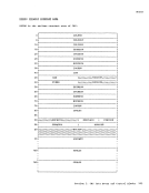
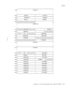
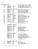
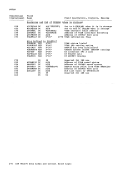
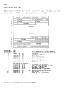
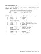
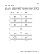
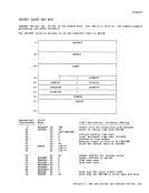
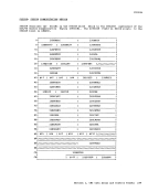
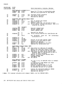
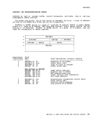
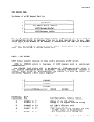
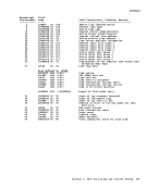
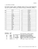
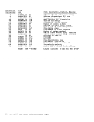
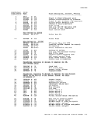
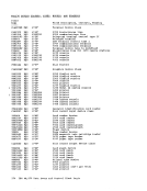
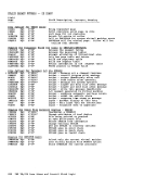
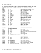
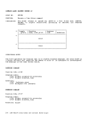
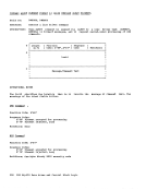
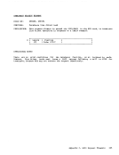
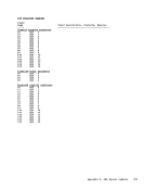
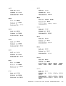
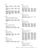
tDRREC DDRREC is used in the SVC 76-initiated error recording process for tYFe 60 tlSD dumF restore (DDR) dynamic device reallocation The reallocation recerds contain the replacement of the virtual "FROM" and "TO" control unit addresses (CUI) by the real addresses of the real DlSD devices. 0 8 10 is 20 28 30 38 Hexadecimal Displacement ------------ 0 2 3 4 5 6 8 C 10 18 20 26 2C 2D 30 34 35 38 DDRKEYB DDRDTEB DDRVOL1 DDRVOL2 DDRDEV1 DDRDEV2 Field Balle DDRKEYB DS DDRSWS1 DD DDRSWS2 DS DDRSWS3 DS DDRRECBT DS DDRSPE1 DS DDRDTEB DS DDRTftEB DS DDRCPlD DS I I D*1 I/D*2/I/D*3/I/t*4/1//tDRSPE1////////1 DDRCPlD nnll"lnl:l (cont.) ID*5 ID*6 1H 1C D*1 1C D*2 1C D*3 1C D*4 1H 1F 1F 2F DtBTftEB tDRVCL2 tDRCU11 tDRCU12 Field Description, Contents, Beaning Type and operating system Switch byte Reserved lBB use Reserved for IBM use Reserved for lBB use Reserved for lBB use Date' Time Processor identification and model number Dependn! Rgta DDRJOB DS DDRVOL1 DS DDRVOL2 DS DDRDEVP1 DS DDRCU11 DS DDRDEV1 DS DDRDEVP2 DS DDRCUA2 DS DDRDEV2 DS DDRSlZE EQU 81 61 61 11 D*5 31 41 11 D*6 31 41 (*-DDRREC) Job using FROft device Voluae serial FROB device Voluae serial TO device Device identification of FRCB DlSD Primary CUI of FROB device Device type FROB Device identification TO DASD Primary CUI of TO device Device type of TO device DDR record size Section 1. CP Data Areas and Centrol Blocks 19