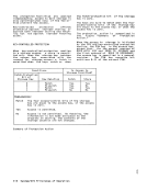
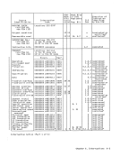
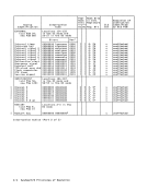
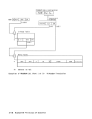
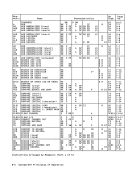
channel, and main-storage location can
be in only one configuration at a time.
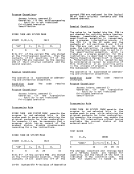
MAINSTORAGE Main storage, which is directly address
able, provides for high-speed processing
of data by theCPUs and channels. Both
data and programs must be loaded into
main storage from input devices before
theycan be processed. The amount of
main storage available on the system
depends on the model, and, depending on
the model, the amount in the configura
tion may be under control of model
dependent configuration controls. The
storage is available in multiples of
2K-byte blocks. When either TESTBLOCK or the storage-key 4K-byte-block facili
ty is installed, storageis available in multiples of 4K-byte blocks. At any
instantin time, all CPUs and all chan
nels in the configuration have access to
the same blocks of storage and refer to
a particular block of main-storage
locations by using the same absolute
address.
Main storage may include a faster-access
buffer storage, sometimes called a
cache. EachCPU may have an associated
cache. The effects, except on performance, of the physical construction and
the use of distinct storage media are
not observable by the prograM.
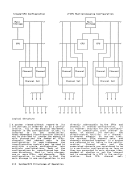
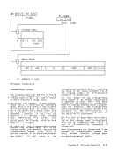
The central processing unit(CPU) is the
controlling center of the system. It
contains the sequencing and processing
facilities for instruction execution,
interruption action, timing functions,initial program loading, and other
machine-related functions.
The physical implementation ofthe CPU may differ among models, but the logical
function remains the same. The result
of executing an instruction is the same
for each model, providing that the
program complies with the compatibility
rules.
TheCPU, in executing instructions, can
process binary integersand floating
point numbers of fixed length, decimal
integers of variable length,and logical
information ofeither fixed or variable
length.Processing may be in parallel
orin series; the width of the process
ingelements, the multiplicity of the
shifting paths, and the degree of simul
taneity in performing the different
types of arithmetic differ from oneCPU ~ to another without affecting the logical
results.
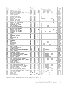
Instructions which theCPU executes fall
into five classes: general, decimal,
floating-point, control, andI/O instructions. The general instructions
are used in performing binary integer
arithmetic operations and logical,
branching, and other nonarithmetic oper
ations. Thedecimal instructions
operate on data in the decimal format,
and the floating-point instructions on
data in the floating-point format. The
privileged control instructions and theI/O instructions can be executed only
when theCPU is in the supervisor state;
the semiprivileged control instructions
can be executed in the problem state,
subject tothe appropriate authorization
mechanisms.
To perform its functions, theCPU may
use a certain amount of internal
storage. Although this internal storage
may use the same physical storage medium
as maln storage, it is not considered
part of main storage and is not address
able by programs.
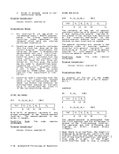
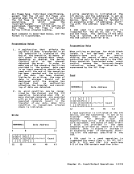
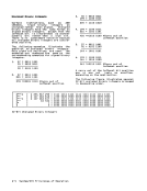
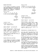
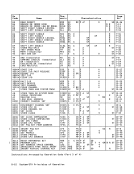
TheCPU provides registers which are
available to programs but do not have
addressable representationsin main
storage. They include the current
program-status word(PSW), the general
registers, the floating-point registers,
the control registers, the prefixregis ter, and the registers for the clock
comparator and theCPU timer. Each CPU in an installation provides access to a
time-of-day(TOO) clock, which may be
local to thatCPU or shared with other CPUs in the installation. The instruc
tion operation code determines which
type of register is to be usedin an
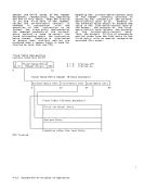
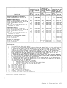
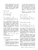
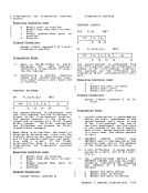
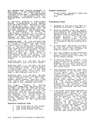
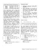
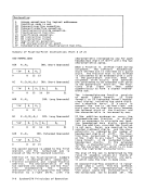
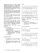
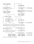
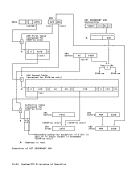
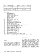
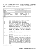
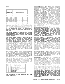
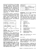
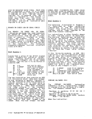
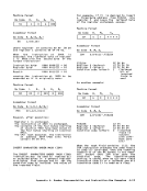
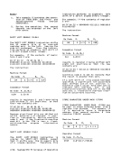
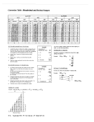
operation.See the figure "General, Floating-Point, and Control Registers" later in this chapter for the format of
those registers.PSW The program-status word (PSW) includes the instruction address, condition code,
and other information used to control
instruction sequencing and to determine
thestate of the CPU. The active or
controllingPSW is called the current PSW. It governs the program currently being executed.
TheCPU has an interruption capability,
which permits theCPU to switch rapidly
toanother program in response to excep tional conditions and external stimuli.
Whenan interruption occurs, the CPU places the current PSW in an assigned storage location, called the old-PSW location, for the particular class of
interruption. TheCPU fetches a new PSW from a second assigned storage location.
This newPSW determines the next program
to be executed. When it hasfinished processing the interruption, the inter- Chapter 2. Organization 2-3
be in only one configuration at a time.
MAIN
able, provides for high-speed processing
of data by the
data and programs must be loaded into
main storage from input devices before
they
main storage available on the system
depends on the model, and, depending on
the model, the amount in the configura
tion may be under control of model
dependent configuration controls. The
storage is available in multiples of
2K-byte blocks. When either TEST
ty is installed, storage
instant
nels in the configuration have access to
the same blocks of storage and refer to
a particular block of main-storage
locations by using the same absolute
address.
Main storage may include a faster-access
buffer storage, sometimes called a
cache. Each
cache. The effects, except on perform
the use of distinct storage media are
not observable by the prograM.
The central processing unit
controlling center of the system. It
contains the sequencing and processing
facilities for instruction execution,
interruption action, timing functions,
machine-related functions.
The physical implementation of
function remains the same. The result
of executing an instruction is the same
for each model, providing that the
program complies with the compatibility
rules.
The
process binary integers
point numbers of fixed length, decimal
integers of variable length,
information of
length.
or
ing
shifting paths, and the degree of simul
taneity in performing the different
types of arithmetic differ from one
results.
Instructions which the
into five classes: general, decimal,
floating-point, control, and
are used in performing binary integer
arithmetic operations and logical,
branching, and other nonarithmetic oper
ations. The
operate on data in the decimal format,
and the floating-point instructions on
data in the floating-point format. The
privileged control instructions and the
when the
the semiprivileged control instructions
can be executed in the problem state,
subject to
mechanisms.
To perform its functions, the
use a certain amount of internal
storage. Although this internal storage
may use the same physical storage medium
as maln storage, it is not considered
part of main storage and is not address
able by programs.
The
available to programs but do not have
addressable representations
storage. They include the current
program-status word
registers, the floating-point registers,
the control registers, the prefix
comparator and the
time-of-day
local to that
tion operation code determines which
type of register is to be used
operation.
those registers.
and other information used to control
instruction sequencing and to determine
the
controlling
The
which permits the
to
When
interruption. The
This new
to be executed. When it has